Printed circuit boards (PCBs) are used in numerous industries to control the electronic functions of products or applications. They provide structural support as they allow the electronic components to become connected. These components are connected using a variety of methods including conductive pathways, signal traces, or tracks. These traces, tracks, and pathways are etched and laminated into the non-conductive substrate using copper sheets.
Some PCBs may have multiple layers containing a conductive material and dielectric materials, which include flexible PCBs and rigid-flex PCBs as well. The circuit board could have anywhere from 3 up to 40 layers depending on the application and its functions. The layers with the conductive material need to connect and allow components to reach the conductive material so signals can move through the circuit board. To accomplish this, holes are drilled into the circuit board at certain depths. After a hole is drilled, a manufacturer may perform etch-back.
PCB Through hole plating
Standard PCB Holes
There are different types of holes drilled into circuit boards. Standard PCB holes consist of through holes, blind vias, buried vias, and micro vias.
- Through holes: Drilled holes that go through all the layers conductive and dielectric layers of the PCB from one side to the other.
- Blind vias: Drilled holes stretching from one external PCB layer into part of the circuit board without going through the other side.
- Buried vias: Holes only through the internal layers of the circuit board without going through either external PCB layer.
- Microvias: Small holes (diameter less than 0.006 inches) made using a laser rather than a drill that only spans two layers of the circuit board.
The outline should be drawn with a line of any width starting at 0, 0. The line should be exact in all X, Y coordinated and dimensioned for verification. We often find critical errors where the numeric dimension does not match the outline. All dimensions are verified within the CAD tool. Determining the drill location starts position within the outline for one. All holes are based off an X and a Y coordinate and consecutive coordinates from that first drilled location to the next.
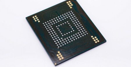
When drilling a hole through the entire printed circuit board, the hole itself may be plated or non-plated. Plated through holes (Figure 1) consists of using copper to plate the surface of the board and through the holes to improve the conductive nature of electronic components with the conductive materials between the dielectric layers. However, the resin used to adhere the multiple board layers together may smear along the holes during drilling which can impact the electronic signals from components and conductive layers. There may also be small bits of dielectric debris remaining in the holes.
While some applications will not have their signals impacted by the resins or dielectric debris, industries such as military, aerospace, and medical require high signal performance at all times. Due to this requirement, manufacturers may perform an etch-back process for multilayer flexible PCBs and multilayer rigid-flex PCBs.
PCB Etch-back
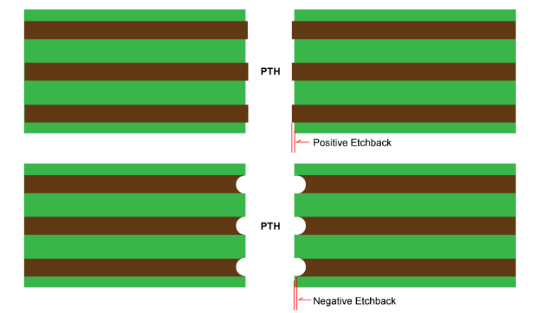
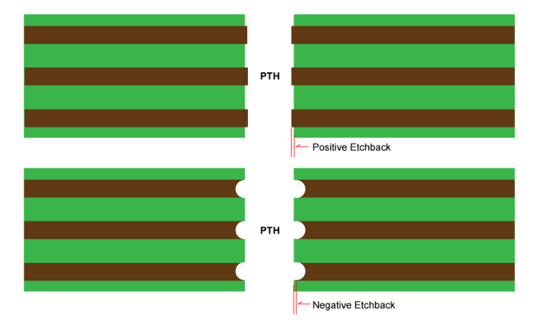
PCB Through hole plating. PCB manufacturers use a process called etch-back to remove the debris and resin smear within through holes. Also called desmearing, the etch-back process occurs before the copper plating method. Etchback removes a certain amount of the conductive layer or the dielectric layer depending on the methods used. Two methods used to etch back the layers are called micro-etch and plasma etch (Figure 2). Micro etch is used for negative etch-back techniques while plasma etches are performed for positive etch-back techniques.
Negative Etch-back
PCB Through hole plating. Negative etch-back (Figure 3) removes (etches) the copper land so it becomes recessed back from the through the hole more than the dielectric materials. A micro etch process is used by applying a copper etchant, which is a ferric chloride solution. The PCB is submerged into this etchant, or the etchant is sprayed into the circuit board as it removes only from 0.001″ to 0.0005″ of copper, based on IPC6013 classes. The drilled holes become desmeared and then the holes become plated.
Negative etch-back is a traditional method used in PCB manufacturing. It is cost-effective and a reliable process that works for many applications. However, negative etch-back may lower the performance of the PCB due to the removal of the copper conductive material, which could create inner layer separation. In addition, air pockets may become trapped inside.

Positive Etchback
Positive etch-back (Figure 4) takes off the non-conductive dielectric layer between the copper conductive layer. This process uses a plasma etch technique with the use of a plasma chamber as the amount of dielectric material that becomes removed is carefully controlled.
All three sides of the copper become exposed due to the removal of the dielectric material and resins as it protrudes into the through hole. The method allows copper plating to occur on all three sides of the conductive copper layer. IPC6013 requirements for positive etch-back state that 0.001″ to 0.08″ of copper is to be exposed when etch-back is specified during PCB development.
Positive etch-back costs more than negative etch-back. However, the method provides higher levels of PCB reliability and may be a requirement for certain industries such as medical, aerospace, and military. A drawback of positive etch-back is that it may create rough holes that lead to through-hole cracks and cause excessive stresses that create foil cracks.

Golden Margins –Entire Range of Touchscreen Products
We hope you found these touchscreen or panel PC fundamentals informative. Goldenmargins offers a broad selection of Industrial Touchscreen Monitors and Touch Panel PCs in various sizes and configurations, including medical touch screens, sunlight-readable touch screens, open-frame touch screens, and waterproof touch panels, as well as other unique touch screen or panel PC designs. You can learn more about our services HERE or by calling us at +86 755 23191996 or sales@goldenmargins.com